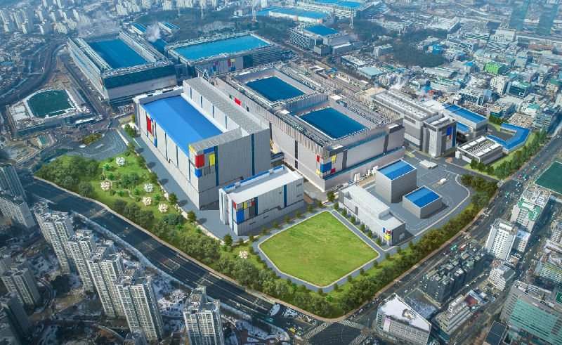
 Samsung has announced that its has completed development of 5-nanometer (nm) FinFET process technology. This comes after it announced the readiness and its initial production of 7nm process, its first process node with EUV lithography technology in October. It provided commercial samples of the industry’s first EUV-based new products and started mass production of 7nm process early this year. Compared to 7nm, Samsung’s 5nm FinFET process technology provides Up to 25% increase in logic area efficiency with 20% lower power consumption or 10% higher performance as a result of process improvement to enable more innovative standard cell architecture. Customers to fully leverage Samsung’s highly sophisticated EUV technology EUV lithography in metal layer patterning and reduces mask layers while providing better fidelity, similar to the predecessor Reuse of all the 7nm intellectual property (IP) to 5nm. Thereby 7nm customers’ transitioning to 5nm will greatly benefit from reduced migration costs, pre-verified design ecosystem, and consequently shorten their 5nm product development. Samsung also announced that it is collaborating with customers on 6nm, a customized EUV-based process node, and has already received the product tape-out of its first 6nm chip. Samsung foundry’s EUV-based process technologies are currently being manufactured at the S3-line in Hwaseong, Korea. It will expand ...
Tuesday, 16 April 2019
Samsung completes development of EUV-based 5nm FinFET process technology
Samsung has announced that its has completed development of 5-nanometer (nm) FinFET process technology. This comes after it announced the readiness and its initial production of 7nm process, its first process node with EUV lithography technology in October. It provided commercial samples of the industry’s first EUV-based new products and started mass production of 7nm process early this year. Compared to 7nm, Samsung’s 5nm FinFET process technology provides Up to 25% increase in logic area efficiency with 20% lower power consumption or 10% higher performance as a result of process improvement to enable more innovative standard cell architecture. Customers to fully leverage Samsung’s highly sophisticated EUV technology EUV lithography in metal layer patterning and reduces mask layers while providing better fidelity, similar to the predecessor Reuse of all the 7nm intellectual property (IP) to 5nm. Thereby 7nm customers’ transitioning to 5nm will greatly benefit from reduced migration costs, pre-verified design ecosystem, and consequently shorten their 5nm product development. Samsung also announced that it is collaborating with customers on 6nm, a customized EUV-based process node, and has already received the product tape-out of its first 6nm chip. Samsung foundry’s EUV-based process technologies are currently being manufactured at the S3-line in Hwaseong, Korea. It will expand ...
-
Here are the social profile links that I have worked on for Backlinks https://docs.google.com/presentation/d/1gAvVQYafqO_jWsSIz3N95Sy3q5KAx...
-
Yi technology, the company which is backed by Xiaomi recently launched products like Yi Home Camera 3, Yi Action Camera, Yi Home Security C...
-
Micromax just launched Bharat GO, the company's first Android Oreo (Go Edition) smartphone in India, in partnership with Airtel. It was...

